- 您现在的位置:买卖IC网 > Sheet目录481 > MTP3055V (ON Semiconductor)MOSFET N-CH 60V 12A TO-220AB
�� �
�
�MTP3055V�
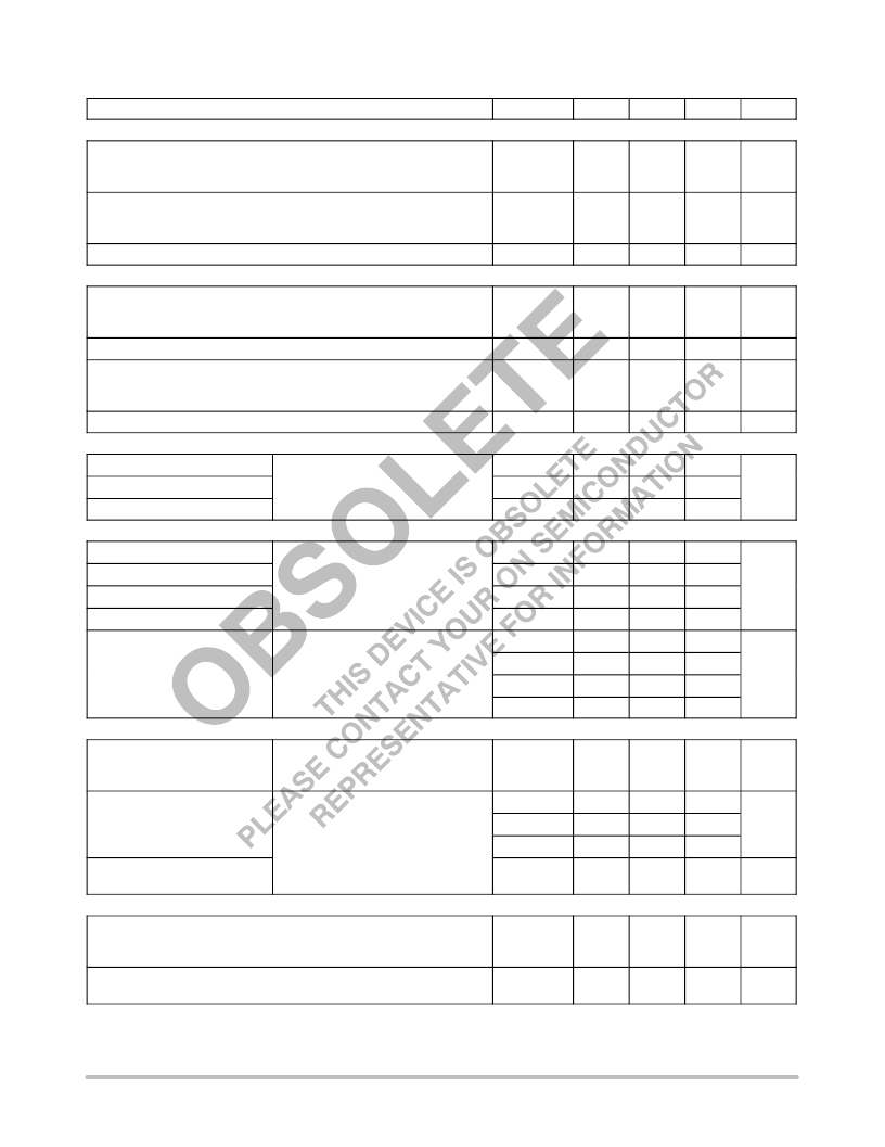
�ELECTRICAL� CHARACTERISTICS� (T� J� =� 25� °� C� unless� otherwise� noted)�
�Characteristic�
�Symbol�
�Min�
�Typ�
�Max�
�Unit�
�OFF� CHARACTERISTICS�
�Drain� ?� Source� Breakdown� Voltage�
�(V� GS� =� 0� Vdc,� I� D� =� 250� μ� Adc)�
�Temperature� Coefficient� (Positive)�
�Zero� Gate� Voltage� Drain� Current�
�(V� DS� =� 60� Vdc,� V� GS� =� 0� Vdc)�
�(V� DS� =� 60� Vdc,� V� GS� =� 0� Vdc,� T� J� =� 150� °� C)�
�Gate� ?� Body� Leakage� Current� (V� GS� =� ±� 20� Vdc,� V� DS� =� 0)�
�V� (BR)DSS�
�I� DSS�
�I� GSS�
�60�
�?�
�?�
�?�
�?�
�?�
�65�
�?�
�?�
�?�
�?�
�?�
�10�
�100�
�100�
�Vdc�
�mV/� °� C�
�μ� Adc�
�nAdc�
�ON� CHARACTERISTICS� (Note� 1)�
�Gate� Threshold� Voltage�
�(V� DS� =� V� GS� ,� I� D� =� 250� μ� Adc)�
�Temperature� Coefficient� (Negative)�
�Static� Drain� ?� Source� On� ?� Resistance� (V� GS� =� 10� Vdc,� I� D� =� 6.0� Adc)�
�Drain� ?� Source� On� ?� Voltage� (V� GS� =� 10� Vdc)�
�(I� D� =� 12� Adc)�
�(I� D� =� 6.0� Adc,� T� J� =� 150� °� C)�
�Forward� Transconductance� (V� DS� =� 7.0� Vdc,� I� D� =� 6.0� Adc)�
�V� GS(th)�
�R� DS(on)�
�V� DS(on)�
�g� FS�
�2.0�
�?�
�?�
�?�
�?�
�4.0�
�2.7�
�5.4�
�0.10�
�1.3�
�?�
�5.0�
�4.0�
�?�
�0.15�
�2.2�
�1.9�
�?�
�Vdc�
�mV/� °� C�
�Ohm�
�Vdc�
�mhos�
�DYNAMIC� CHARACTERISTICS�
�Input� Capacitance�
�Output� Capacitance�
�Reverse� Transfer� Capacitance�
�(V� DS� =� 25� Vdc,� V� GS� =� 0� Vdc,�
�f� =� 1.0� MHz)�
�C� iss�
�C� oss�
�C� rss�
�?�
�?�
�?�
�410�
�130�
�25�
�500�
�180�
�50�
�pF�
�SWITCHING� CHARACTERISTICS� (Note� 2)�
�Turn� ?� On� Delay� Time�
�t� d(on)�
�?�
�7.0�
�10�
�ns�
�Rise� Time�
�Turn� ?� Off� Delay� Time�
�Fall� Time�
�(V� DD� =� 30� Vdc,� I� D� =� 12� Adc,�
�V� GS� =� 10� Vdc,�
�R� G� =� 9.1� Ω� )�
�t� r�
�t� d(off)�
�t� f�
�?�
�?�
�?�
�34�
�17�
�18�
�60�
�30�
�50�
�Gate� Charge�
�(See� Figure� 8)�
�(V� DS� =� 48� Vdc,� I� D� =� 12� Adc,�
�V� GS� =� 10� Vdc)�
�Q� T�
�Q� 1�
�Q� 2�
�?�
�?�
�?�
�12.2�
�3.2�
�5.2�
�17�
�?�
�?�
�nC�
�Q� 3�
�?�
�5.5�
�?�
�SOURCE� ?� DRAIN� DIODE� CHARACTERISTICS�
�Forward� On� ?� Voltage� (Note� 1)�
�Reverse� Recovery� Time�
�(See� Figure� 15)�
�Reverse� Recovery� Stored�
�Charge�
�(I� S� =� 12� Adc,� V� GS� =� 0� Vdc)�
�(I� S� =� 12� Adc,� V� GS� =� 0� Vdc,� T� J� =� 150� °� C)�
�(I� S� =� 12� Adc,� V� GS� =� 0� Vdc,�
�dI� S� /dt� =� 100� A/� μ� s)�
�V� SD�
�t� rr�
�t� a�
�t� b�
�Q� RR�
�?�
�?�
�?�
�?�
�?�
�?�
�1.0�
�0.91�
�56�
�40�
�16�
�0.128�
�1.6�
�?�
�?�
�?�
�?�
�?�
�Vdc�
�ns�
�μ� C�
�INTERNAL� PACKAGE� INDUCTANCE�
�Internal� Drain� Inductance�
�(Measured� from� contact� screw� on� tab� to� center� of� die)�
�L� D�
�?�
�3.5�
�?�
�nH�
�(Measured� from� the� drain� lead� 0.25� ″� from� package� to� center� of� die)�
�4.5�
�Internal� Source� Inductance�
�(Measured� from� the� source� lead� 0.25� ″� from� package� to� source� bond� pad)�
�L� S�
�?�
�7.5�
�?�
�nH�
�1.� Pulse� Test:� Pulse� Width� ≤� 300� μ� s,� Duty� Cycle� ≤� 2%.�
�2.� Switching� characteristics� are� independent� of� operating� junction� temperature.�
�http://onsemi.com�
�2�
�发布紧急采购,3分钟左右您将得到回复。
相关PDF资料
MTP36N06V
MOSFET N-CH 60V 32A TO-220AB
MTP50P03HDL
MOSFET P-CH 30V 50A TO-220AB
MTPD1346-010
PIN DIODE 1300NM FLAT 2.8MM TO46
MTPD1346-030
PIN DIODE 1300NM FLAT 2.8MM TO46
MTPD1346-100
PIN DIODE 1300NM FLAT 2.8MM TO46
MTPS1065PT
VISIBLE RED POINT SOURCE EMITTER
MTPS1065WC
VISIBLE RED POINT SOURCE EMITTER
MTPS3085CP
EMITTER IR POINT SOURCE
相关代理商/技术参数
MTP3055V
制造商:Fairchild Semiconductor Corporation 功能描述:MOSFET
MTP3055V_L86Z
功能描述:MOSFET TO-220
RoHS:否 制造商:STMicroelectronics 晶体管极性:N-Channel 汲极/源极击穿电压:650 V 闸/源击穿电压:25 V 漏极连续电流:130 A 电阻汲极/源极 RDS(导通):0.014 Ohms 配置:Single 最大工作温度: 安装风格:Through Hole 封装 / 箱体:Max247 封装:Tube
MTP3055VL
功能描述:MOSFET 60V Single N-Ch RoHS:否 制造商:STMicroelectronics 晶体管极性:N-Channel 汲极/源极击穿电压:650 V 闸/源击穿电压:25 V 漏极连续电流:130 A 电阻汲极/源极 RDS(导通):0.014 Ohms 配置:Single 最大工作温度: 安装风格:Through Hole 封装 / 箱体:Max247 封装:Tube
MTP3055VL
制造商:Fairchild Semiconductor Corporation 功能描述:N CHANNEL MOSFET 60V 12A ((NW)) 制造商:Fairchild Semiconductor Corporation 功能描述:N CHANNEL MOSFET, 60V, 12A, TO-220
MTP3055VL_Q
功能描述:MOSFET 60V Single N-Ch
RoHS:否 制造商:STMicroelectronics 晶体管极性:N-Channel 汲极/源极击穿电压:650 V 闸/源击穿电压:25 V 漏极连续电流:130 A 电阻汲极/源极 RDS(导通):0.014 Ohms 配置:Single 最大工作温度: 安装风格:Through Hole 封装 / 箱体:Max247 封装:Tube
MTP30N06VL
制造商:MOTOROLA 制造商全称:Motorola, Inc 功能描述:TMOS POWER FET 30 AMPERES 60 VOLTS RDS(on) = 0.050 OHM
MTP30N08M
制造商:MOTOROLA 制造商全称:Motorola, Inc 功能描述:POWER FIELD EFFECT TRANSISTOR
MTP30P06
制造商:MOTOROLA 制造商全称:Motorola, Inc 功能描述:TMOS POWER FET 30 AMPERES 60 VOLTS RDS(on) = 0.080 OHM